Semiconductors

One of the core challenges that Rapidus will face when it kicks off volume production of chips on its 2nm-class process technology in 2027 is lining up customers. With Intel, Samsung, and TSMC all slated to offer their own 2nm-class nodes by that time, Rapidus will need some kind of advantage to attract customers away from its more established rivals. To that end, the company thinks they've found their edge: fully automated packaging that will allow for shorter chip lead times than manned packaging operations. In an interview with Nikkei, Rapidus' president, Atsuyoshi Koike, outlined the company's vision to use advanced packaging as a competitive edge for the new fab. The Hokkaido facility, which is currently under construction and is expecting to begin equipment installation...

TSMC Jumps Into Silicon Photonics, Lays Out Roadmap For 12.8 Tbps COUPE On-Package Interconnect
Optical connectivity – and especially silicon photonics – is expected to become a crucial technology to enable connectivity for next-generation datacenters, particularly those designed HPC applications. With ever-increasing bandwidth...
9 by Anton Shilov on 4/26/2024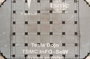
TSMC's System-on-Wafer Platform Goes 3D: CoW-SoW Stacks Up the Chips
TSMC has been offering its System-on-Wafer integration technology, InFO-SoW, since 2020. For now, only Cerebras and Tesla have developed wafer scale processor designs using it, as while they have...
2 by Anton Shilov on 4/26/2024
TSMC Preps Cheaper 4nm N4C Process For 2025, Aiming For 8.5% Cost Reduction
While the bulk of attention on TSMC is aimed at its leading-edge nodes, such as N3E and N2, loads of chips will continue to be made using more mature...
6 by Anton Shilov on 4/25/2024
TSMC 2nm Update: N2 In 2025, N2P Loses Backside Power, and NanoFlex Brings Optimal Cells
Taiwan Semiconductor Manufacturing Co. provided several important updates about its upcoming process technologies at its North American Technology Symposium 2024. At a high level, TSMC's 2 nm plans remain...
0 by Anton Shilov on 4/25/2024
TSMC's 1.6nm Technology Announced for Late 2026: A16 with "Super Power Rail" Backside Power
With the arrival of spring comes showers, flowers, and in the technology industry, TSMC's annual technology symposium series. With customers spread all around the world, the Taiwanese pure play...
18 by Anton Shilov on 4/25/2024
TSMC Posts Q1'24 Results: 3nm Revenue Share Drops Steeply, but HPC Share Rises
Taiwan Semiconductor Manufacturing Co. this week released its financial results for Q1 2024. Due to a rebound in demand for semiconductors, the company garned $18.87 billion in revenue for...
11 by Anton Shilov on 4/19/2024
ASML Patterns First Wafer Using High-NA EUV Tool, Ships Second High-NA Scanner
This week ASML is making two very important announcements related to their progress with high numerical aperature extreme ultraviolet lithography (High-NA EUV). First up, the company's High-NA EUV prototype...
13 by Anton Shilov on 4/18/2024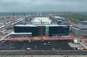
Samsung To Receive $6.4 Billion Under CHIPS Act to Build $40 Billion Fab in Texas
Samsung Electronics this week was awarded up to $6.4 billion from the U.S. government under the CHIPS and Science Act to build its new fab complex in Taylor, Texas...
5 by Anton Shilov on 4/16/2024
TSMC to Receive $6.6B Under US CHIPS Act, Set to Build 2nm Fab in Arizona
TSMC has entered into a preliminary agreement with the U.S. Department of Commerce, securing up to $6.6 billion in direct funding and access to up to $5 billion in...
23 by Anton Shilov on 4/8/2024
Rapidus to Get $3.9 Billion in Government Aid for 2nm, Multi-Chiplet Technologies
Rapidus, a Japan-based company developing 2nm process technology and aiming to commercialize it in 2027, will receive a huge government grant for its ongoing projects. The Japanese government will...
10 by Anton Shilov on 4/2/2024
Construction of $106B SK hynix Mega Fab Site Moving Along, But At Slower Pace
When a major industry slowdown occurs, big companies tend to slowdown their mid-term and long-term capacity related investments. This is exactly what happened to SK hynix's Yongin Semiconductor Cluster...
8 by Anton Shilov on 3/23/2024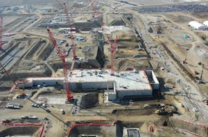
Intel to Receive $8.5B in CHIPS Act Funding & Further Loans To Build US Fabs
Intel and the United States Department of Commerce announced on Wednesday that they had inked a preliminary agreement under which Intel will receive $8.5 billion in direct funding under...
20 by Anton Shilov on 3/20/2024
NVIDIA's 'cuLitho' Computational Lithography Adopted By TSMC and Synopsys For Production Use
Last year, NVIDIA introduced its cuLitho software library, which promises to speed up photomask development by up to 40 times. Today, NVIDIA announced a partnership with TSMC and Synopsys...
21 by Anton Shilov on 3/18/2024
ASML Delivers First 2nm-Generation Low-NA EUV Tool, the Twinscan NXE:3800E
Our avid readers tend to look at microelectronics made using leading edge process technologies, which in case of Intel means usage of High-NA extreme ultraviolet (EUV) lithography a couple...
2 by Anton Shilov on 3/13/2024
Marvell's 2nm IP Platform Enables Custom Silicon for Datacenters
Marvell this week introduced its new IP technology platform specifically tailored for custom chips for accelerated infrastructure made on TSMC's 2nm-class process technologies (possibly including N2 and N2P). The...
0 by Anton Shilov on 3/8/2024
Intel to Hold Webinar to Discuss Long-Term Vision for Foundry, Separating Fab and Design Reporting
As Intel prepares to move its fabs into its new Intel Foundry business, it will change the way it reports results in the coming months. To discuss the company's...
1 by Anton Shilov on 3/7/2024
Arm and Samsung to Co-Develop 2nm GAA-Optimized Cortex Cores
Arm and Samsung this week announced their joint design-technology co-optimization (DTCO) program for Arm's next-generation Cortex general-purpose CPU cores as well as Samsung's next-generation process technology featuring gate-all-around (GAA...
3 by Anton Shilov on 2/22/2024
IFS Reborn as Intel Foundry: Expanded Foundry Business Adds 14A Process To Roadmap
5 nodes in 4 years. This is what Intel CEO Pat Gelsinger promised Intel’s customers, investors, and the world at large back in 2021, when he laid out Intel’s...
29 by Ryan Smith on 2/21/2024
GlobalFoundries to Receive $1.5 Billion In Funding from U.S. CHIPS Act
The United States Department of Commerce and GlobalFoundires announced on Monday that the US will be awarding GlobalFoundries with $1.5 billion in funding under the CHIPS and Science Act...
5 by Anton Shilov on 2/20/2024
GlobalFoundries: Clients Are Migrating to Sub-10nm Faster Than Expected
When GlobalFoundries abandoned development of its 7 nm-class process technology in 2018 and refocused on specialty process technologies, it ceased pathfinding, research, and development of all technologies related to...
26 by Anton Shilov on 2/14/2024


